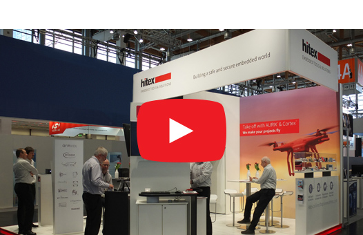


For many years, Hitex has been a leading supplier of innovative and reliable tools for embedded engineers. In addition, Hitex supports customers on a consulting basis in all phases of their development projects, from concept to system realisation.
We work closely with leading semiconductor and compiler manufacturers in order to support all the latest product and software releases, as well as industry standards.